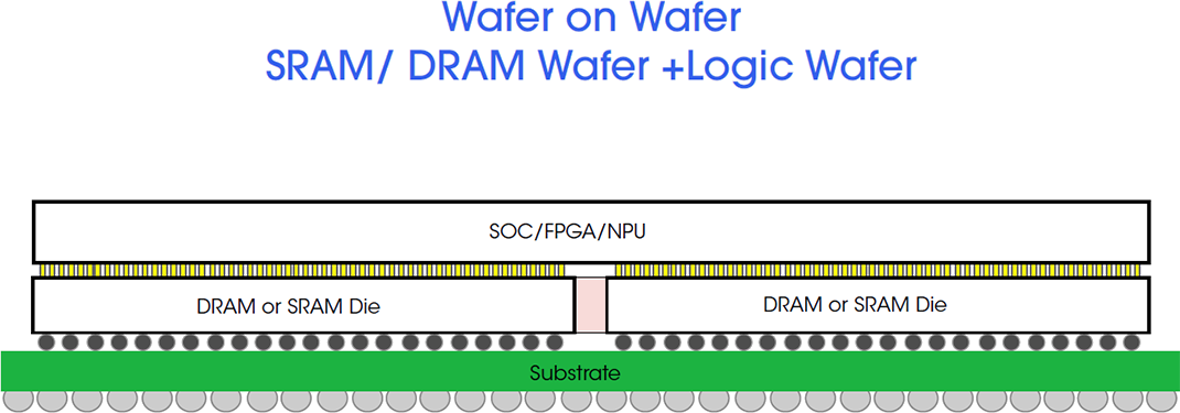
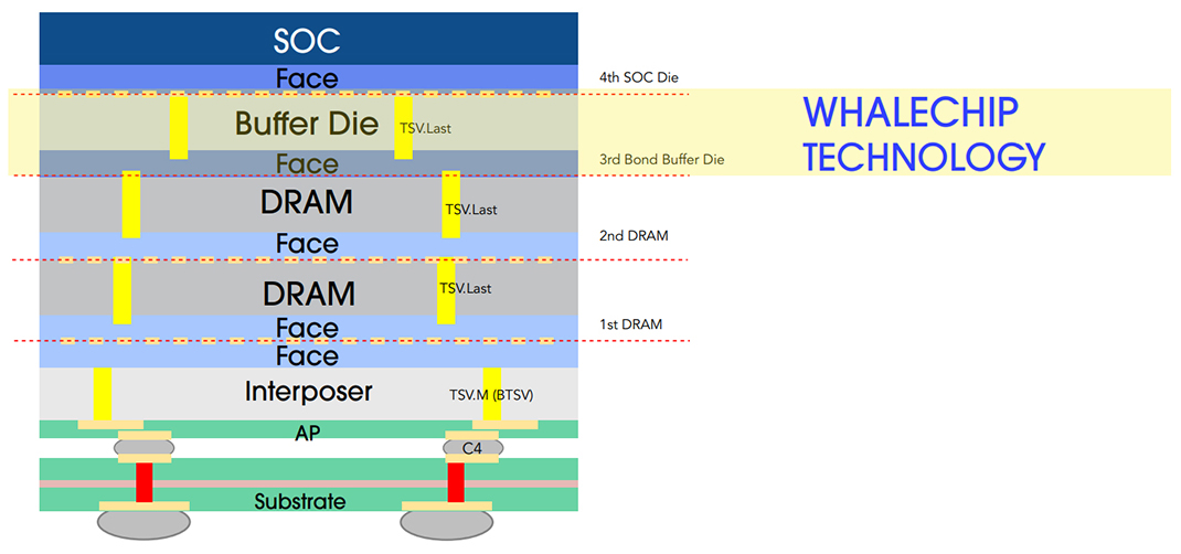
TECHNOLOGY
WoW 3DIC Technology
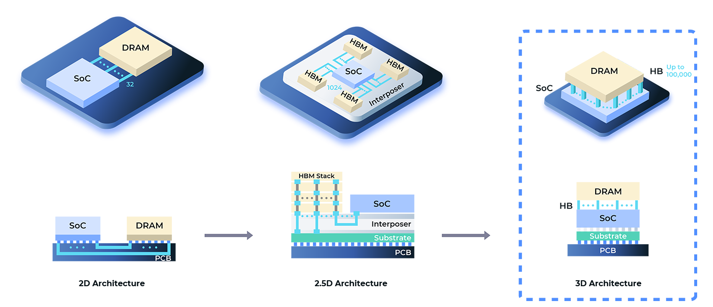
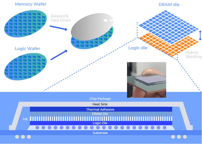
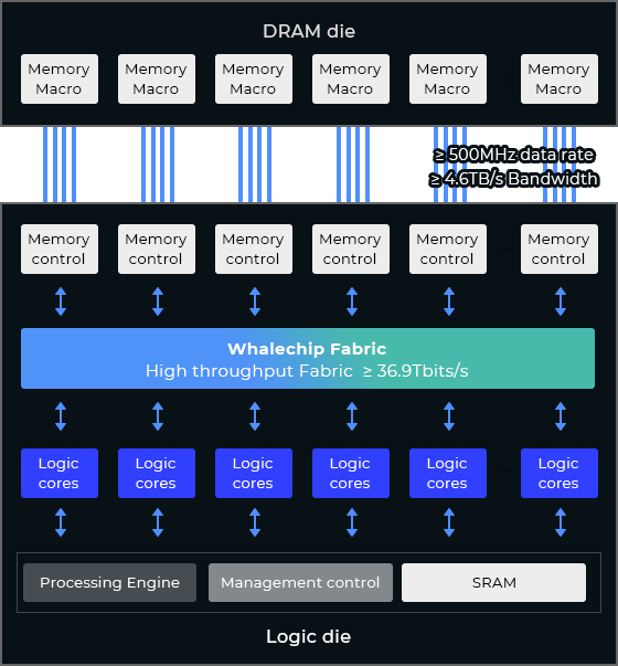
WHALECHIP’s Wafer-on-Wafer (WoW) 3DIC technology adopts advanced Hybrid Bonding at the wafer level to vertically integrate chips of different types, architectures, and even process nodes. Compared to the typical external DDR/HBM connections used in 2.5D CoWoS packaging, WoW 3DIC significantly increases interconnect density and quantity, eliminates the need for PHY interfaces, and greatly shortens signal paths. These enhancements reduce system power consumption and overall area, dramatically increase data bandwidth, overcome memory bottlenecks, and significantly enhance overall computing performance.
WoW 3DIC :
Next-Gen technology
To meet high data flow requirements in AI/ HPC applications, the 2.5D packaging approach (CoWoS) uses HBM placed around the logic chip with 1,024 pins connecting (each HBMx) to the SoC.
Placing hundreds of chips on an interposer for 2.5D packaging is technically challenging due to space limitations.
Whalechip WoW is true 3D stacked with 100,000 up pins, delivering over 10-100 times higher bandwidth, reduced power consumption, and space-saving benefits.
*
WHALECHIP WoW 3DIC 1.0
Integrates logic and memory directly on two wafers via Hybrid Bonding(WoW).
Solved the Von Neumann bottleneck That has plagued the HPC/AI Chip developers.
*
*
WHALECHIP WoW 3DIC Technology/Product Roadmap
*
WHALECHIP OPUS:
3D Stacked Wafer-Scale Integration Solution

To achieve higher overall computing performance and memory bandwidth, we developed a wafer-scale stacked heterogeneous integrated 3DIC. This cutting-edge technology enables ultra-high interconnect density, reduced latency, and scalable performance for future chip designs.

*
WHALECHIP WoW 3DIC 2.0

Advanced 3DIC Architecture for Next-Gen Computing

In WHALECHIP’s WoW 3DIC 2.0 architecture, stacking the SoC on top of 3D TSV DRAM helps reduce the SoC die area and minimizes the area overhead caused by TSV integration, enabling a more cost-efficient design for edge AI devices. Additionally, the top-layer SoC placement also contributes to improved system thermal performance

WHALECHIP Buffer Die Solution :

The WHALECHIP Buffer Die serves as a centralized control core with integrated memory controller functionality. It incorporates a DRAM controller, refresh controller, test and repair modules—such as MBIST, Repair, and ECC—as well as AXI and APB interfaces, providing comprehensive memory access control.
This architecture not only offloads memory management tasks from the SoC but also enables high-speed, low-power data exchange through close-proximity vertical stacking (with the SoC on top and Buffer Die in the middle), delivering a more efficient and optimized memory subsystem for high-performance computing (HPC) and edge AI applications.

*